
Scientific journal
European Journal of Natural History
ISSN 2073-4972
ИФ РИНЦ = 0.204
OPTIMIZATION OF THE SCHEME OF AN ELECTRIC WELDING DEVICE

Secondary power supplies of an inverter type inverted for electrowelding devices [1...6] are widely known. These devices have some disadvantage, namely, the current amplitude in inverter power transistors intended for electrowelding devices is great and makes about one third of the value of the loading current, i.e. in an electric act .This disadvantage is due to the fact that with a view of stabilization of the "burning" mode of an electric are and its easy ignition elaborators of these devices are compelled to make the synchronizing transformer secondary winding voltage extremely high in comparision with the arc voltage. The value of it is approximately 100 V. accordingly, at the initial network voltage 220 V the straightened and smoothed up to Um = 220∙ ≈ 300 V voltage at the inverter input makes the transformation factor 300/100 = 3, at this value the current amplitude in inventer power transistors is egual to one third of the arc current. At the same time we know that actually the arc voltage does not exceed the value of 25 V at air welding and is considerably less at welding in CO2 and argon. This disadvantage i.e. too high voltage results, first, in the increase of inverter transistors capacity and cost and, second, in the grouth of losses in - them.
The principle of the new device is explained in Figure, where the secondary power supply is shown schematically. The device consists of controlled network rectifier, transistor inverter 2, connected by an input with direct current terminals of controlled network rectifier 1, synchronizing transformer 3, a primary winding 4 of which is connected with diode rectifier 6, its direct current terminals being connected with a transistor inverter output. Secondary winding 5 of synchronizing transformer 3 is connected with diode rectifier 6, the direct current terminals are connected to load 8 activating an electrode and a welding arc via smoothing choke 7 in series with it.
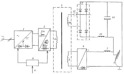
They make the basic power supply. Network rectifier I and transistor inverter 2 are controlled by typical system 9, current task signal i3 being supplied to its output. Besides a synchronizing transformer is eguipped with additional secondary winding 10 connected with diode bridge alternating current diagonal 12 via a filter in series, diode bridge being an additional power supply. The diode bridge direct current diagonal is connected with load 8 in parallel to the basic power supply via a Г-shaped filter. The Г-shaped filter contains choke 13 in series between a diode bridge terminal 12 and a corresponding load terminal and filter condenser 14 in parallel with load 8. It allowed to make the additional power supply perform functions of ignition and stabilization of an electric arc in a zone of small current, to lower the synchronizing transformer basic secondary winding voltage up to 35 V and, thus, to reduce the inverter transistor current amplitude considerably (approximately 3 times).
In conventional secondary power supplies the synchronizing transformer secondary winding voltage is about 100 V. The inverter voltage powered by a single-phase network (~220 V) is approximately 300 V, the transformation factor 300/100 is 3 and, accordingly, the current amplitude in inverter transistors is 1/3 of a load current , e.g. at the load current of 200 A the transistor current (in amplitude) of the devices under consideration will be 200/3 ≈ 67 A.
As in the device elaboratore the voltage is reduced up to 35 V, the inverter transistors current amplitude will be 100/35 ≈ 2,85 times as low . If is rather important due to the fact that power transistor or compound transistor modules, first, make an essential part of the total cost of a device; second decrease of the current reduces losses. The losses in an additional power supply are negligibly small as it is used for a short period of time. One should note that if it is necessary to use the welding device in CO2 or argon environment, one should just disconnect additional secondary winding 10 of synchronizing transformer, as in these modes rigid external characteristic is reguired and we don´ t need to increase the voltage to " ignite" an arc. Thus, the offered device does not lack universally and, simultaneously has essential advantage in air welding mode, transistor current in envertery 2 is 3 times as low in comparision with a current amplitude in conventional devices, and ignition conditions of an electric act are improved as an electrode contact with a part being welded is accompanied by a forced energy discharge, this energy having been saved up in filter condenser 14.
References
- DS-200 AL-Technotron . Russia, a catalogue, 1995.
- Transpoket // Ausria, a catalogue. - 1995-96.
- Invertec. V-130-S-Lincoln-USA- 1997.
- Yastolin YmbH - Yermany.Kraftzwerg- 1994-96.
- Secondary power sumply. Palent 2242835 of 20.12.2004 / Аuthors L.T. Magazinnik, A.G. Magazinnik.
- Magazinnik A.G., Magazinnik L.T., Magazinnik G.G. Correction of the capacity factor of secondary power Supplies // Electrical engineering. - 2001. - Vol.5. - P. 40-42.
Библиографическая ссылка
Magazinnik L.T OPTIMIZATION OF THE SCHEME OF AN ELECTRIC WELDING DEVICE // European Journal of Natural History. 2011. № 3. ;URL: https://world-science.ru/en/article/view?id=28021 (дата обращения: 28.07.2026).