
Scientific journal
European Journal of Natural History
ISSN 2073-4972
ИФ РИНЦ = 0.204
MULTIFUNCTIONAL MEMORY CIRCUITS OF MARAKHOVSKY

Throughout the world, the search for new circuit-based solutions of elementary memory circuits with qualitatively new properties continues [1–5]. Unfortunately, all the works on the tunable memory scheme under consideration were carried out due to tunable excitation functions and outputs based on the RS trigger, which have fundamental limitations [6]:
1. They all work in the automaton discrete time ti (i = 1, 2. …, n,…);
2. The basic memory scheme (RS-trigger) for known triggers does not allow you to rebuild the work of memorized states;
3. All these devices are described by the Mealy and Moore automata, which determine the sequential nature of the operation of the devices;
4. The transition in memory circuits occurs in one variable x(t);
5. The principle of program management proposed by Charles Bebbage does not allow the simultaneous processing of general and local information and determines the division of information into only two parts.
In connection with these fundamental limitations of the class of monofunctional memory circuits (triggers), multifunctional memory schemes are proposed based on new principles and methods of structural organization.
The principle of the structured organization of multifunctional memory circuits (MFIS) is that n logical elements OR-NOT (AND-NOT) are used, which are divided into m (m < n) groups. The outputs of the elements of one group are not associated with the inputs of their group of logical elements. They are connected to the inputs of the elements of other groups of the memory scheme according to one of the defined laws (for example, with the inputs of all other logical elements or the inputs of only elements of two, three, etc. of m groups of elements). One of the free inputs of each i-th element is connected to the inputs of the setting input bus, and the second of the free inputs of each i-th element is connected to the inputs of the memory bus that stores the input bus. The introduction of an additional saving input bus in the memory scheme and the creation of groups of logical elements in a group of more than one was a fundamentally new phenomenon in the development of multifunctional memory circuits.
The principle of memorizing states in an MFIS is that the input signals that establish xi(t) that arrive at the nodes of the setting input bus uniquely determine the output active values of at least one logical element of the i-th group.
The output active values of the installed element through their output structural bonds keep the output values of other elements of the memory circuit inverted, which in turn through the inverse structural connections confirm the established output values of the logic elements when one of the conserved sets of input signals supplied by the conserving input bus. These set values of the state of the memory circuit a(Δ) are stored due to the state preservation functions δe until the next input xi(t) input signal arrives [7].
The use of state conservation functions δe in monofunctional Miley and Moore automata (also in memory circuits (triggers)) was not considered, because all triggers kept their states only with one passive input signal e(Δ), which was called an “empty word of zero length” although this function physically existed. In automatic discrete time, there was no length (interval Δ) for it, and under its influence no single transition from one state to another was realized. But this input signal e(Δ) has always been taken into account by the developers of memory circuits.
Definition 1. The MFIS will be called a single-level multifunctional elementary automaton (MEA) with a complete transition system and a complete output system for each of the re (re > 1) state conservation functions δe.
MEAs can be functionally represented as re single-level elementary automata, each of which remembers all its states only with one of the various corresponding sets of input signals that preserve ej(Δ) ( ) [7].
Method of microstructural synthesis of elementary multifunctional memory circuits
Consider a method of microstructural synthesis, which allows us to construct an asynchronous MFIS class L from the logical elements of a functionally complete system.
We use the combination scheme OR-NOT, which realizes this function:
 , (1)
, (1)
where f(a) – is a function of an arbitrary input signal coming from the output of an element of another group for storing the state in the MFIS;
f(x) – is a function of an arbitrary set of input signal хi(t);
f(e) – is a function of an arbitrary saving еj(Δ) set of the input signal.
The combination scheme (1) is called a basic automaton with one state or simpler than a basic automaton (BA). The simplest BA are logical elements of the AND-OR-NOT, OR-NOT or NAND type.
The method of microstructural synthesis of asynchronous MFIS of class L consists of the following algorithm. We take n BA and divide them into m (m < n) groups. The BA in each i-th group (i = 1, 2, ..., m) has no feedback, because their output nodes do not join the input nodes of the BA of this i-th group. The outputs of the BA of the i-th group are respectively connected directly or through the OR (AND) separation scheme or directly to the inputs f(a) of all BAs of the other groups.
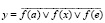
One of the free inputs zi of each i-th BA is connected to the inputs of the setting input bus ШХ, and the second of the free inputs ui of each i-th BA is connected to the inputs storing the input bus ШЕ of the memory circuit. Input nodes zi can receive input xi(t) input signals, and input ei(Δ) inputs can be input sequentially one by one for one clock cycle Ti (Ti = ti + Δi). Stable output signals at the output nodes yj of the BA correspond to the shifted states aj(T) of the MFIS, where aj(T) = ai(t) + ai(Δ). The shift of the output signal yj(T) is equal to the delay of two logic elements, which is necessary to establish a stable output state in the memory circuit.
The x(t) input signals of the MFIS unambiguously establish a certain state aj(t) of the memory circuit. The excitation function δx in an elementary automaton can be described in vector form:
 (2)
(2)
The value of the binary set at the input nodes zj of the multifunctional memory scheme, under the action of the input signal setting x(t), is characterized by the fact that only at the input nodes of the logical elements (BAj) of one i-th group, the input signal can have a value equal to the passive signal 0 (1 ) On at least one logical element (BAj) of this i-th group. At the input nodes of logic elements (BAj) of other groups, the values of the input signal must be equal to the active signal 1 (0). The MFIS stored signal еj(Δ) can memorize one of the states aj(Δ) defined by the state block πj, predetermined by the setting input signal xi(t). The function δe of conservation of a state in an elementary automaton can be described in vector form:
 (3)
(3)
The value of the binary set at the input nodes uj of the MFIS under the action of the saving e(Δ) input signal is characterized by the fact that at least two MFIS groups at the input nodes of the BA have input signals whose value is equal to the passive signal 0 (1). The number K of storage states for a given e(Δ) input signal is equal to the number of groups in the MFIS, at the inputs of which the value of the input signal at node uj is equal to the passive signal 0 (1). Thus, the value of the number K can vary depending on the input signals e(Δ) saving from 2 to m. The state ai of the MFIS is identified with the state of the values of the output signals yj BAj of only one group if at least one of the output signals yj of this group is equal to the active signal 1 (0). The unit value of the output signal yj in this group is called the MFIS, because this output signal yj acts on the BAj of other groups, setting on them output signals yj equal to the logical zero. The characteristic number Ki of the storage states of the i-th group is calculated by the formula:
Ki = 2R –1, (4)
where R is the BA number in the i-th group of the MFIS.
The number Ki of the storage states of the i-th group of the MFIS is a block of μi states. The transition from the state ak to the state as in the block of μi states is possible with a change in the e(Δ) input signal. Such a transition is called enlarged. The function δy of the coarse transition can be represented in vector form:
 (5)
(5)
Table 1
Setting the block n states of monofunctional memory circuits
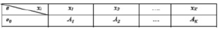
Table 2
Specifying the state matrix of multifunctional memory circuits
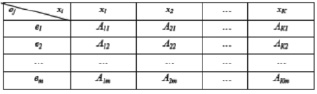
Thus, the number of memory states of an MFIS can be represented in a matrix form, where the rows of the matrix determine the blocks of πj states that are remembered for the corresponding input signals retaining ej(Δ), and the matrix columns are the states μi blocks that are set by the corresponding setting xi(t) input signals. A single-valued transition from the state ai in the state ak of the πj state block (in the matrix row) is performed under the influence of the input signals establishing the xi(t) and the enlarged transition to the new state in the μi state block – under the influence of the preserving e(Δ) Input signals trigger circuits and SMEs have only one block of π states. This characteristic indicates that monofunctional memory circuits (triggers and SMEs) is a particular case of the MFIS. Consider tables of tasks for monofunctional (Table 1) and multifunctional (Table 2) memory schemes, which supports this conclusion.
The function φ of the outputs in the MFIS depends on the setting input word p = x, e, which establishes and stores the states a. In this case, two cases are possible: when the function δe of conservation of state (3) or the function δy of the coarse transition (5) is realized.
The function φ1 of the outputs, which depends on the state of the automaton a(Δ – 1) and sets the input signal x(t), characterizes the first-order automaton and in the vector form has the form:
у(t) = φ1 [a(Δ – 1), х(t)]. (6)
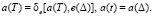
The function φ2 of the outputs depends on the state a(t) of the state and on the stored a(Δ) state, which characterizes the automaton of the second kind and in the vector form has the form:
у(Т) = φ2 [a(t), a(Δ)]; a(t) = a(Δ), (7)
or
у(Т) = φ2 [a(Т)], а(Т) = a(t) U a(Δ). (8)
The function φ2 outputs ensures that the set state a(T) is maintained for a continuous cycle time T.
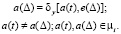
The function φ3 of the outputs in the MFIS depends on the set a(t) state and on the stored input signal e(Δ) and which can be represented in vector form as follows:
y(Δ) = φ3 [a(t), e(Δ)]. (9)
The function φ3 outputs characterizes automata of the third kind, which determines the direction of the output signal y(Δ) as a function of the saving signal e(Δ).
Description of elementary multifunctional memory circuits
The most famous binary elementary memory circuits are triggers based on the RS-trigger [4-6], which is a particular case of the MFIS [2]. Such schemes are characterized by three main parameters: M – the number of stable states a, each of which corresponds to a certain output signal of the memory circuit y2 (T); rx – is the number of setting input signals x(t) and rе – is the number of conserved input signals e(Δ), which are formally associated with the MFIS structure. The basic MFIS structures created on NAND or NOR logical elements are called basic automata (BA), and their parameters are determined by the proposed formulas.
Memory circuits consist of groups BA (elements), the groups of which are interconnected by feedback circuits, and the characteristic number of memory states Ki in the i-th group is determined by the formula (4). Thus, the number M of stable states a(Δ) of the MFIS stored under the influence of the input signals retaining e(Δ) is determined by the formula:
 (4.10)
where Ki – is the characteristic number of states in the ith group of the MFIS.
The total number rx of different sets of x(t) input signals set by the MFIS is given by:
rx = М + 1, (11)
where M – is the number of stable states of the MFIS, which are conserved;
1 – is an additional set of the input signal that sets xp(t), which uniquely establishes the state ar(t), which is not conserved for any set of the MFIS stored e(Δ) input signal. Such a set of xp(t) input signal in deterministic devices is forbidden [5].
The total number rе of different sets of e (Δ) inputs that are stored in the MFIS can be defined by the formula
 (12)
(12)
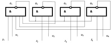
Fig. 1. MFIS class L on the elements of the AND-NOT
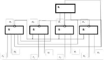
Fig. 2. MFIS class LM on the elements of the AND-NOT
Thus, it becomes clear that two sets of input signals are required for the operation of multifunctional circuits: setting and saving ej(Δ), which enter one clock cycle of T (T = t + Δ). A feature of these two sets of input signals is that the setting xi (t) absorbs the preserving ej(Δ) if they arrive at the same hour.
xі(t) = xі(t) . (13)
Logical elements of one group are connected by their output nodes to the input nodes of all logical elements of other groups. Other inputs of logic elements (at least two) that connect to the corresponding input MFIS buses are used for setting and storing input signals. The output nodes of the logic elements are connected to the output line of the MFIS.
Let us consider an example of the synthesis of the functional scheme of an MPSE on the elements AND-NOT of two classes L and LM.
An important functional advantage of MFIS over flip-flops and SMBs is the possibility of reconstructing the structure of the memory states during operation for one machine clock T, otherwise it can be said that an increase in the degree of freedom from 1 to re is determined.
Conclusion
Multifunctional memory circuits have the advantage over the basic binary memory scheme of the RS-flip-flop. MISPs reduce the hardware costs per stored state; increase the functionality by realigning the structure of state storage and simultaneously processing the levels of hierarchical information represented as sets of input-preserving signals e(Δ) as general and local information represented as sets of input signals x(t) in one machine clock cycle T.
Библиографическая ссылка
Marakhovsky L.F. MULTIFUNCTIONAL MEMORY CIRCUITS OF MARAKHOVSKY // European Journal of Natural History. 2018. № 5. ;URL: https://world-science.ru/en/article/view?id=33933 (дата обращения: 25.06.2026).