
Scientific journal
European Journal of Natural History
ISSN 2073-4972
ИФ РИНЦ = 0.204
OPTIMIZATION OF THE CONTROL OVER A TRANSISTOR INVERTER SCHEME

A singlephax bridge transistor inverter can be used in varios secondary power supplies in a power range from tens of watts up to several kilowatts, instance in electrowelding devices, singlephas plasmotrones, electronic voltage stabilizers etc.
Secondary power supplies with inverters are divided into two groups: with a controllable inverter and with a noncontrollable one [1].
A singlephax noncontrollable bridge transistor inverter described in [1] is connected with an adjustable network rectifier with its own control and adjustment system via a direct current diagonal.The disadvantage of this device is that the unverter power transistor control system contains besides a typical oscillator of a given frequency and a synchronizing transformer,a shaper of porosity of controlling impulses operating on the principle of pulse-width modulation and an optoelectronic modular power transistor with an optoelectronic outcome. If makes the device more complicated and expensive as a whole.
A simplified scheme of a singlephas noncontrollable bridge transistor inverter is shown in Figure.
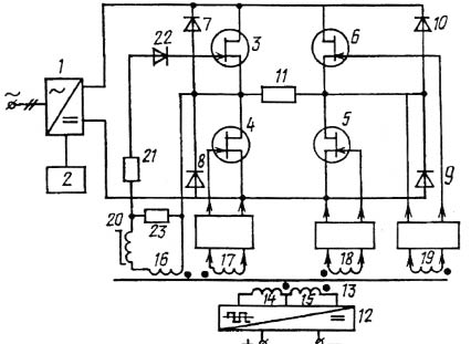
The device 1 contains adjustable network rectifier 1 based on the scheme of a semicontrollable bridge with a smoothing condenser at the output. The controlling input of network rectifier 1 is connected with the output of the controlling and adjustment system 2 and a singlephax noncontrollable bridge transistor inverter direct current diagonal is connected with the outcome of a network rectifier 1. The power part of the inverter contains four power transistor 3, 4, 5, 6 arranged as a bridge and shunted by the opposite diode bridge 7, 8, 9, 10. Load 11 is connected to an alternating current diagonal. The control system of the inverter consist of autooscillator 12, synchronizing transformer 13 connected with autooscillator 13 via a primary winding. A primary winding of synchronizing oscillator 13 has two identical semiwindings 14 and 15 connected properly and which have an additional average terminal. All three terminals of a primary winding are connected with the outcome of autooscillator 12, it is a typical construction. Four secondary windings 16, 17, 18, 19 according to the number of power transistor are built in pairs and opposite in control channels and in pairs in accordance with each other in diagonal channels of transistor bridge 3, 4, 5, 6. If is also a typical construction. The porosity shaper of controlling pulses and galvanic outcome circuits are combined in each of four identical channels controlling power transistors and contain quickly saturated choke 20, resistor 21, limiting the current and diod 22 connected with the appropriate power transistor (e.g. transistor 3) in conducting direction. All connections are in series. For simplicity one controlling channel is shown in Fig.2. The emitter of power transistor 3 is connected with one of the terminals of the appropriate secondary winding 16 of synchronizing transformer 13, and a free terminal of quickly saturated choke 20 is connected with the second terminal of secondary winding 16 of synchronizing transformer 13. Besides, the emitter of power transistor 3 and the common point of quickly saturated choke 20 and resistor 21 limiting the current are shunted by ballast resistor 23.
The required output capacity of autooscillator 12 when the voltage of secondary windings 16, 17, 18, 19 of synchronizing oscillator 13 is (3...5) will be 2∙(3...5)iδ, where iδ is the current of unloching of power transistor: iδ = ik/α, where α - is the strengthening factor of a power transistor, and ik is the collector current (the «locing» current is negligibly small). It follows that if ik = 30 A, α = 15. The output capacity of autooscillator 12 is only
![]() (1)
(1)
no preliminary amplification is reguired in comparison with shapers with optoelectronic outcome , where current is measured in milliamperes and amplification is necessary.
Quickly saturated choke 20 providing the necessary interval τ is calculated when τ and the voltage of a secondary voltage of synchronizing transformer 13 are known by the formula
U = 4,44∙f∙B∙S∙W, (2)
where U ≈ (3...5)V, f ≈ 5∙105 kc (when τ ≈ 1⋅10-6 с), В ≈ 0,2 ТS (for ferrite cores). S is the crossection of a core in m2, W is the number of turns of a choke. Calculations show that a choke with a winding of (4...7) turns on a core S ≈ 5 mm2 provides the necessary interval τ,that is the size and the mass of a 3, quickly saturated choke are rather small.
Thus, rather complex and expensive part of the device in the structure of the width-pulse modulator and power transistor modules with optoelectronic galvanic outcome is replaced by an elementary circuit consisting of a tiny quickly saturated choke, a diode and two resistors controlled by one channel and common power transistors instead of expensive power transistor modules.
References
- Pryanishnikov B.A. Electronics. - St. Petersburg, 1998. - 400 p.
- The patent 2233536 Russian Federation.A single phas noncontrollable bridge transistor inverter / L.T. Magazinnik, G.G. Magazinnik, V.P. Shingarov. B.I. vol. - 21, 27.07.04.
Библиографическая ссылка
Magazinnik L.T OPTIMIZATION OF THE CONTROL OVER A TRANSISTOR INVERTER SCHEME // European Journal of Natural History. 2011. № 3. ;URL: https://world-science.ru/en/article/view?id=28020 (дата обращения: 19.06.2026).