

A single-phax bridge transistor inverts are applied in various secondary power supplies, e. g. in audio and video devices in electrowelding devices etc.
Welding devices of an inverter type containing power supplies (a network rectifier), an actual inverter, a matching power transformer connected to an inverter via a primary winding and to loading [1] via a secondary winding and a diode rectifier are widely known.
Inverters in the installations listed are carried out under a single-stroke scheme that leads to inefficient use of a matching power transformer and a smoothing choke, to the necessity of having a transformer with an air clearance in the core and, consequently, to the increase of magnetization current and losses. The specified lacks are appreciably compensated by frequency increase of the converter, however losses in a semi-conductor part of the inverter (power transistor, diodes, snubbers) grow and the requirement to semiconductor base frequency characteristics increase. It results in the growth of cost.
A two-stroke scheme of the inverter (e.g. a semi-bride one [2]) is deprived of the abovementioned lacks of one-stroke schemes but provides an inefficient use of switching condensers and the main thing , a condenser built into an inverter power circuit causes nonlinearity of the external characteristics of a device. In [2] a two-stroke bridge scheme of an inverter where the efficiency of a switching transformer is 4 times as higher in comparison with a semi bridge scheme is presented , but a condenser built in series with a secondary winding of a power matching transformer results in voltage resonance and disables the scheme.
A «classical» two-stroke bridge inverter scheme with an inverse diode bridge [3] has the best characteristics. But when used for transformer loading it posesses the lacks stated above. The control of the inverter is usually carried out by means of pulse-width modulator, the typical one- and two-stroke schemes are given in [2, 3].
In any two-stroke scheme of an inverter without condensers an asymmetry in the output voltage curve in a power circuit is inevitable because of technical disorder of parameters of separate inverter elements and, as a consequence, a constant component in output voltage may appear. The latter in its turn, makes us to employ a power matching transformer with an air clearance. Dimensions and magnetization current of a transformer are increased accordingly and advantages of a two stroke-scheme over a one-stroke one are brought to naught.
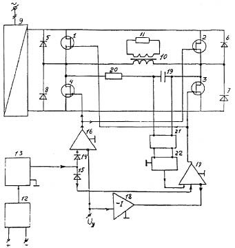
The device scheme allowing to exclude a constant component in the inverter output voltage is presented in Figure.
In the power part the scheme contains a bridge inverter as a single- phax transistor bridge (1, 2, 3, 4) shunted by inverse diode bridge 5, 6,7, 8 which is connected to power supply 9 via a direct current diagonal and to loading 11 via an alternating current diagonal and power matching transformer 10. The control system is a typical two-stroke width-pulse modulator containing two-stroke autooscillator 12, its output being connected to sawtooth voltage two-stroke oscillator input 13. This voltage arrives at the first inputs of comparators 16, 17: plus arrives at the first input of comparator 16, minus at the first input of comparator 17 via dividing diodes 14 and 15.
The control signal Uy arrives directly at the second input of comparator 16 and via logic inverter 18 at the second input of comparator 17. Output of comparators16 and 17 are connected to corresponding inputs of diagonal pairs of transistors 2, 4 and 1, 3. For simplicity galvanic outcome and intermediate strengthening elements between comparators output and control inputs of transistors 1, 2, 3, 4 are not shown in Fig.1. Thus, the scheme in Fig.1 repeats the scheme described in [3]. Some additional elements are included : a R-C circuit consisting of condenser 19 and resistor 20 in series is built in in parallel with a primary winding of transformer 10. Integrator 22, the output of which is connected to the third input of comparator 17 is connected to a condenser via galvanic outcome unit 21.
It is necessary to notice that all additional elements including condenser 19 and resistor 20 are low-current. At the same time the device offered allows us to realize the advantages of the bridge scheme to the full: reduction of the dimensions of a power matching transformer - 2-4 times; reduction of the dimensions of a smoothing choke-twice (in case of a d. c. loading); reduction of a magnetizing current and, accordingly, losses.
References
- Tranporket-Austria, the Catalogue of 1995-96.
- Pryanishnikov V.A. Electronics. - St.-Petersburg, 1998. - P. 374.
- Sources of secondary power supplies. Under the editoship of Y.I. Konev. - M.: Radio and Communication, 1983.
- The patent 2223590 Russian Federation. A bridge inverter / L.T. Magazinnik, A.G. Magazinnik. - B.I.№.4, 10.02.2004.